Newsroom

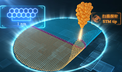
Graphene origami. Schematic of pristine graphene manipulation with a scanning tunnelling microscope. Credit: Chinese Academy of Sciences
It's easier to fold a napkin than a notepad. The potential to manipulate graphite into precise nanostructures using a scanning probe microscope has teased researchers ever since Thomas W. Ebbesen and Hidefumi Hiura first reported accidental tears and folds in their graphite during scanning tunnelling microscope (STM) experiments in the mid-1990s. However, although ensuing studies by various research groups around the world were also able to demonstrate similar origami-like folding of graphite with a scanning probe, they could not command where or how the folds would occur. Now, by replacing the graphite with high-quality graphene nanoislands, researchers in China and the US have finally leveraged the atomic-level control of STM into an origami nanofabrication tool with a comparable level of precision.
"Similar to conventional paper origami, our current work has made it possible to create new complex nanostructures by custom-design folding of atomic layer materials," says Hong-Jun Gao, a researcher at the Chinese Academy of Sciences (CAS) who led this latest work. Alongside Shixuan Du and collaborators at CAS, as well as Vanderbilt University and the University of Maryland in the US, Gao reports how they can fold single layers of graphene with the direction of the fold specified over a range from around the magic angle at 1.1° (where observations of correlated electron behaviour have been causing such a stir) to 60°, with a precision of 0.1°. Their STM manipulations also leave tubular structures at the edges that have one-dimensional structure electron characteristics similar to carbon nanotubes.
"We have demonstrated that through such simple graphene origami we can realize various graphene structures like carbon nanotubes and their intramolecular junctions, which we can generally learn about only from text books," he adds. They list superconductors, Weyl semimetals, and ferromagnetic materials among the fields they expect to benefit from the unprecedented precision of their graphene origami nanofabrication technique.
The pristine single layer advantage
Key to the success of their technique is the quality of the graphene they fold. Most previous experiments attempting to use STM in origami were on graphite with little control over the folds as a result. As Gao points out, "We all know that it is easier to make the art of paper folding with a single paper sheet, as compared with folding piles of papers."
That said this is not the first report of scanning-probe manipulation of graphene. Hannes C. Schniepp and colleagues reported folding graphene with an atomic force microscopy tip in 2008. Their graphene was functionalized and the work concluded "the folding and bending behaviour of the sheets is dominated by pre-existing kink (or even fault) lines consisting of defects and/or functional groups." Later work by Kim Akius and Jan van Ruitenbeek at Leiden University in the Netherlands also operated on graphene but "using the prepatterning in a new way, as a template for folding." Gao and colleagues uniquely operate on pristine graphene letting the STM alone dictate the folding directions and angles. In addition, the STM manipulations are so delicate that even subsequent unfolding and refolding again in different configurations leave no trace of damage on the pristine crystal lattice structure.
To produce well controlled single-atom thick nanoislands for their experiments the researchers bombard highly oriented pyrolytic graphite with hydrogen ions for 10 cycles before annealing them. The whole procedure takes around 10 hours in a vacuum – the cordon bleu of graphene as opposed to fast food – but as the researchers are quick to point out, once these high-quality materials are ready, "the success rate of graphene origami with the assistance of STM is very high and reproducible as demonstrated in our report."
Starting from a single graphene layer, also allows them to create different origami nanostructures by simply modifying the atomic layer itself, such as making a bicrystal graphene island. In future work, Gao and colleagues hope to extend their demonstration of the technique to other 2D materials such as MoS2 and hexagonal boron nitride.
A playground for new discovery
The signatures of delocalized electron behaviour in the electronic properties of their nanostructures is evidence of the high quality of the crystal retained throughout the manipulations. In the twisted bilayer graphene structures produced by folding, the researchers already demonstrate the moiré superlattices that have attracted so much study for understanding the twist-tuned electronic and magnetic properties in bilayer graphene near the magic angle.
In addition, current versus voltage measurements of the tubular structures at the edge reveal van Hove singularities characteristic of one-dimensional structures. The researchers also find the direction of the fold affects the electronic properties of the tubular structures just as for carbon nanotubes, and they detect effects such as peak shifts that they can attribute to interactions with the substrate.
"This [technique] can allow us to immediately explore and test some predicted new physics and device concepts that were otherwise not feasible in the past due to fabrication challenges," he adds.
Schniepp, who led the team behind the first report of folding functionalized graphene with a scanning probe microscope tool, but was not involved with the current work told Physics World how much the high quality of this work impressed him. "The precision with which they repeatedly fold and unfold single-layer graphene at arbitrary angles is remarkable," he says. "It's a beautiful example of how scanning probe techniques cannot only image, but also to manipulate, control and engineer materials at the nano- or even at the atomic scale. I have always been intrigued by the scanning probe techniques and their possibilities, and this work just pushes the state of the art quite a bit further, which I find quite inspiring."
Full details are reported in Science. (Physics World)
