A research team led by HAN Keli from the Dalian Institute of Chemical Physics (DICP) of the Chinese Academy of Sciences, in collaboration with Tonu Pullerits and Khadga Jung Karki from Lund University of Sweden, revealed the charge carrier transport mechanism in perovskite micro-plate via high resolution mapping of photocurrent. Their findings were published in The Journal of Physical Chemistry Letters.
Organometal Halide Perovskites (OHPs) with outstanding optoelectronic properties and cheap synthesis methods have received broad attentions. The remarkable performance of perovskite-based optoelectronic devices is closely related to the long charge carrier diffusion length.
Still, the carrier distribution and transport mechanism in devices with electric field applied are complex and not fully understood. These fundamental issues need to be clarified to further improve the performance of the perovskite-based optoelectronic devices.

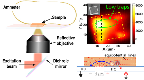
Scanning photocurrent microscopy scheme and photocurrent mapping. (Image by YANG Bin and CHEN Junsheng)
The scientists used CH3NH3(MA)PbBr3 micro-crystals (MCs) as an active material for sensitive photodetectors. It was found that the hole transport length (LD) in the MCs depended on the applied electric field: Under negligible bias, LD was determined by charge carrier diffusion. At higher bias, LD increased and was mainly determined by the drift of the carriers.
Importantly, the PC exhibited a spatial variation, which was mainly due to the inhomogeneous distribution of trap-states in the MCs.
This work was supported by the key research project of National Natural Science Foundation.

86-10-68597521 (day)
86-10-68597289 (night)

52 Sanlihe Rd., Xicheng District,
Beijing, China (100864)

