Scientists at the CAS Institute of Modern Physics (IMP) in Lanzhou, capital of northwest China's Gansu Province, recently made an essential advance in production and investigation of single- and polycrystalline gold nanowires by galvanic replication of ion track templates. Their work has been published by the
Nanotechnology (Vol. 17, 1922-1926, 2006).
Because of its superb electrical and thermal conductivity, and mechanical properties, the gold nanowire is noted for its promising technological applications in nano-electronics, optoelectronics, and chemical and biological sensors. These functions, however, are strongly dependent on the crystallographic and morphological characteristics. By the method of the electrochemical deposition in etched ion-track membranes, both the shape and the crystallinity of nanowires may be under manipulated control.
Supported by Light in Western China Project, a research team headed by Prof. LIU Jie of the IMP has recently succeeded in production of gold nanowires in etched ion-track templates. The polymer membranes are irradiated with swift heavy ions in accelerator, and then etched to obtain pores with controlled density, different shapes, diameters and aspect ratios. Subsequently, these nano-pores are filled with gold in electrochemical deposition process. In this way, the array of gold nanowires ranging from 20 to 100 nm in diameter, in either poly- or single-crystalline structure, is synthesized in the membrane.
The wires possess cylindrical shape, and smooth and homogeneous contour (Fig.1). By varying the deposition conditions, both poly-crystalline (Fig. 2a and 2b) and single-crystalline structure (Fig. 2c) are synthesized. The latter has a [110] preferred orientation while the former features a remarkable ductility (Fig. 2b). By using scanning tunneling microscopy, the research team made an analysis, in which, the grain size of the poly-crystalline wire is about 10 nm (Fig. 3).
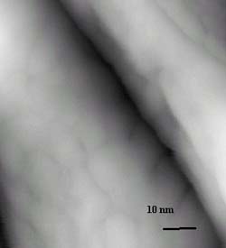
Fig. 3 The poly-crystalline image of the gold nanowires under scanning tunneling microscopy (STM).
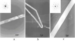
Fig. 2 The images of high-resolution transmission electron microscopy (HRTEM) of poly- and single-crystalline wires. The inset shows selected area electron diffraction (SAED) patterns.
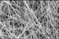
The scanning electron microscopy (SEM) images of the poly-crystalline gold nanowires.
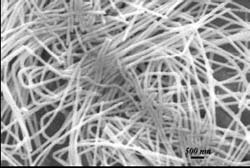
The scanning electron microscopy (SEM) images of the single-crystalline gold nanowires.


