
Prof. PAN Xu's team from the Hefei Institutes of Physical Science of the Chinese Academy of Science, in collaboration with ZHENG Xiaojia from the Chinese Academy of Engineering Physics, and other researchers, discovered the remarkable potential of one-dimensional (1D) δ-phase formamidinium lead iodide (δ-FAPbI3) as an advanced material for X-ray detection.
The results were published in ACS Nano.
Perovskite materials with excellent optoelectronic properties have great potential for direct X-ray detection, with several orders of magnitude higher sensitivity and lower detection limits than current commercial detector materials, and are expected to dramatically reduce the radiation dose rate in radiographic imaging.
However, the preparation of polycrystalline wafers generates a large number of grain boundaries and pores, which leads to severe ion migration and further causes device instability and current drift, severely limiting the imaging resolution of the detectors and future commercial applications.
In this study, the researchers focused on the unique properties of 1D δ-FAPbI3. This yellow phase compound has high ion mobility barriers, low Young's modulus, and exceptional long-term stability.
"We consider it an ideal candidate for high-performance X-ray detection," said YE Jiajiu, a postdoctoral researcher, "especially the dense wafer devices prepared by a cold isostatic pressing process can detect X-rays with high sensitivity and low detection limits."
In addition, the researchers fabricated an X-ray imager with large-sized δ-FAPbI3 wafers integrated on a thin-film transistor (TFT) backplane, realizing two-dimensional multi-pixel X-ray imaging and demonstrating the feasibility of the δ-FAPbI3 wafer detector for ultra-stable imaging applications.
Prof. PAN was optimistic about the future prospects of this technology. "This study provides a new design idea and material selection system for perovskite application in X-ray imaging," he said.
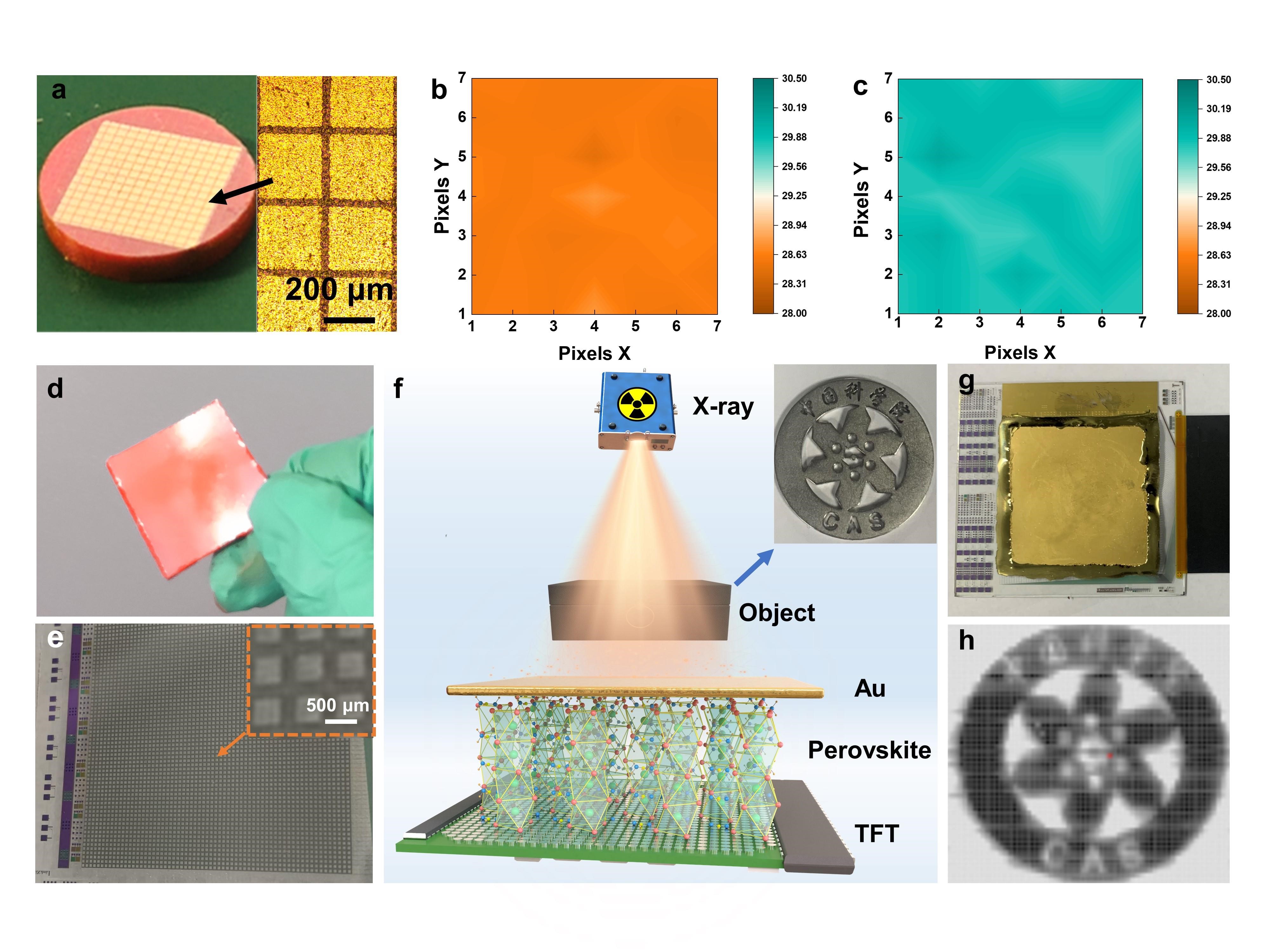
a. 14 × 14 pixel wafer detector; b, c. Bright and dark state mapping; d. 3 × 3 cm δ-FAPbI3 wafer; e. 64 × 64 pixel TFT backplane microstructure; f. Schematic of the X-ray imaging process; g. Flat panel X-ray imaging detector; h. X-ray imaging. (Image by YE Jiajiu)
In a study published in Angew. Chem. Int. Ed., the research group led by Prof. GAO Peng from Fujian Institute of Research on the Structure of Matter of the Chinese Academy of Sciences reported a comprehensive dual-passivation (DP) strategy to effectively passivate the def...
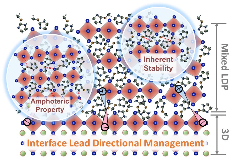
A research team lead by PAN Xu from the Hefei Institutes of Physical Science (HFIPS), cooperating with ZHENG Haiying from Anhui University, have achieved high-efficiency perovskite solar cells by passivating interface defects using new-type low-dimensional perovskite.

86-10-68597521 (day)
86-10-68597289 (night)

52 Sanlihe Rd., Xicheng District,
Beijing, China (100864)
Copyright © 2002 - Chinese Academy of Sciences


