
In a recent paper published in Science Advances, Profs WU Zhou and ZHANG Yuyang from University of Chinese Academy of Science (UCAS) report that by using the mismatched lateral interface between two semiconducting monolayer materials with different lattice constants, a surprising method for growing two-dimensional quantum well superlattices only a few atoms thick was found.
A superlattice is an artificial crystal structure consisting of two or more materials, which are grown alternately on top of each other in a periodic fashion.
Typically, the thickness of each material, or the width of the quantum wells, in the stacking direction of the superlattice is controlled within the range of several nanometers, such that the quantum confinement effect becomes significant allowing intriguing properties to emerge in these artificial structures.
Semiconductor superlattices have thus found important applications in electronics and optoelectronic devices, such as quantum cascade lasers, infrared photodetectors, high electron mobility transistors, high efficiency thermoelectrics, and solar cells.
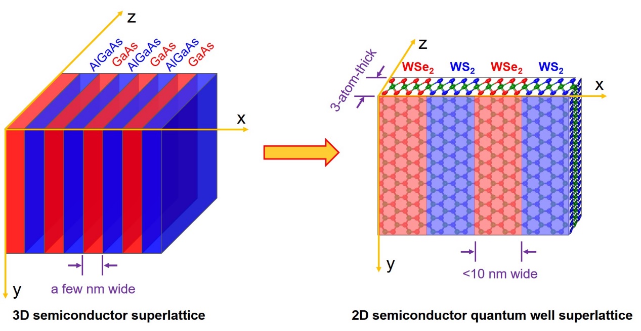
Schematics of three-dimensional and two-dimensional semiconductor superlattices. (Image by WU Zhou)
Compared to the well-established 3D semiconductor superlattice, 2D quantum well superlattices are only a few atoms thick and exhibit an extra degree of the quantum confinement effect in thickness, as schematically shown above.
Constructing such 2D superlattices is challenging due to their atomic thickness. At present, there are several ways to construct such 2D artificial structures. However, these methods still have shortcomings in terms of feature widths.
The results reported by ZHOU and collaborators came as a surprise in the study of two kinds of semiconducting monolayer materials-lateral heterostructures of monolayer tungsten disulfide (WS2) and tungsten diselenide (WSe2), which have about a 4% difference in lattice constants.
With the help of atomic resolution imaging in low-voltage aberration-corrected scanning transmission electron microscopy (STEM), they observed a novel quantum well superlattice structure with a uniform width of 1.2 nanometers and periodicity of about 10 nanometers (see the figures below), and they finally revealed the mystery.

Atomic resolution images of a novel two-dimensional WS2|WSe2 quantum well superlattices with the corresponding structural model on the right. (Image by WU Zhou)
It turns out that the inherent lattice mismatch between the two materials, generates periodic arrays of misfit dislocations (a type of structural defect consisting of connected pairs of 5- and 7-atom rings) in order to release the interfacial strain.
Dislocations, which are considered structural defects, are usually undesired in semiconducting materials. However, in this particular case, their motion drives the growth of this novel two-dimensional quantum well superlattice.
This new misfit-dislocation-driven growth mechanism is expected to be universally applicable to different combinations of two-dimensional materials with lattice mismatch, paving the way to a wide range of two-dimensional quantum-well superlattices with interesting electronic and optical properties.
The research was supported in part by the National Natural Science Foundation of China and the Chinese Academy of Sciences.

86-10-68597521 (day)
86-10-68597289 (night)

52 Sanlihe Rd., Xicheng District,
Beijing, China (100864)
Copyright © 2002 - Chinese Academy of Sciences


