Two-dimensional (2D) layered perovskites (A)2(CH3NH3)n-1MnX3n+1 have recently emerged as an attractive material for applications in photovoltaics and other optoelectronic devices (A is a large aliphatic or aromatic alkylammonium cation working as an insulating layer, M is the metal cation, and X is the halide anion). It has demonstrated that 2D layered perovskite films actually comprised multiple perovskite phases (with various n values from 1, 2, 3 and 4 to near ∞), even though the films were intended to be prepared as a single-phase. This hybrid feature seems to be ineluctable in fabricating 2D films.
However, it's still a burning question that how the different perovskite phases align in the hybrid films. Moreover, it is also unclear whether the band alignment between different phases can induce energy funneling or instead charges separation.
The latter is especially important because it dictates the application of these hybrid 2D perovskite films. Energy funneling is useful for light emitting applications, whereas charge separation would be more beneficial for light conversion or detection.

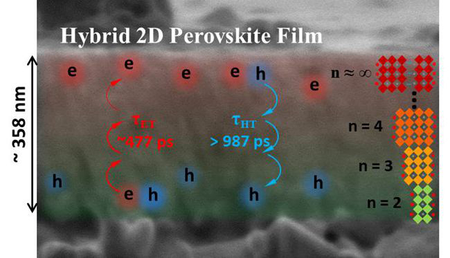
The Hybrid 2D Perpvslite Film (Image by LENG Jing and JIN Shengye)
The research group led by Prof. JIN Shengye in Dalian Institute of Chemical Physics studied the charge carrier dynamics in 2D multi-layered perovskite films, using ultrafast transient absorption and photoluminescence spectroscopy. Researchers found that multiple perovskite phases inside 2D layered perovskite film (including n = 2, 3, 4 and ≈ ∞) naturally align in the order of n along the direction perpendicular to the substrate.
Driven by the band alignment between 2D perovskites phases, researchers observed consecutive photoinduced electron transfer from small-n to large-n phases. And the hole transfers in the opposite direction on hundreds of picoseconds inside the 2D film with the thickness around 358 nm. This internal charge transfer efficiently separates electrons and holes to the upper and bottom surfaces of the films. The phenomenon is a unique property beneficial for applications in photovoltaics and other optoelectronics devices.
The related results were published in Journal of the American Chemical Society (DOI: 10.1021/jacs.6b12581). This work is financially supported by Ministry of Science and Technology (2016YFA0200602) and National Nature Science Foundation of China (2013CB834604).

86-10-68597521 (day)
86-10-68597289 (night)

52 Sanlihe Rd., Xicheng District,
Beijing, China (100864)

