
Solar radiation is by far the most abundant source for clean and sustainable energy. Effectively harvesting solar energy to drive semiconductor materials for the production of other energy forms, such as chemical energy, electricity and thermal energy, is an ideal tactic to conquer the growing worldwide energy crisis. The full harvest of solar energy by semiconductor in light conversion requires such a material to simultaneously absorb diverse spectrum ranges of solar radiation and collect photo-generated electrons and holes separately.
To address this, a team led by
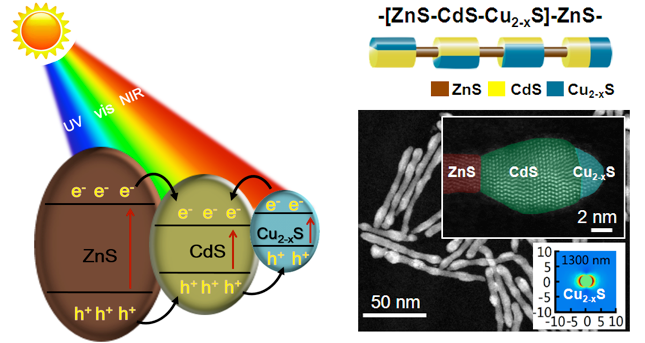
Left: Energy band alignment and the flow of photo-generated carriers in ZnS-CdS-Cu2-xS nanosystem. The hybrid ternary ZnS-CdS-Cu2-xS is able to effectively absorb the ultraviolet (UV), visible (vis) and near infrared (NIR) light. The flow of photo-generated electrons is guided to the conduction band of CdS in this hybrid system, while the hole carriers are mostly accumulated at the valence band of Cu2-xS. Right: Schematic illustration depicting the ternary ZnS-CdS-Cu2-xS heteronanorods and TEM and HAADF-STEM images of heteronanorods. Inset shows the high-resolution HAADF-STEM image, ZnS: red, CdS: green, Cu2-xS: cyanine./Coutesy by Material Views
This multiple selective integration of p-type and n-type sulfides with variable band gaps but free of noble metals may provide a new horizon for enhanced full-spectrum solar energy absorption and efficient charge separation in the conventional semiconductor photoelectric field. This designed semiconducting hybrid system can be regarded as an important step toward a new generation of efficient solar cells covering the rainbow colors and beyond.
The results were published in
The research project is sponsored by the National Basic Research Program of China, the National Natural Science Foundation of China and the Chinese Academy of Sciences. (Material Views)

86-10-68597521 (day)
86-10-68597289 (night)

52 Sanlihe Rd., Xicheng District,
Beijing, China (100864)
Copyright © 2002 - Chinese Academy of Sciences


