
Recently, researchers from Institute of Microelectronics of Chinese Academy of Sciences (IMECAS) carried out new technology on the defect behavior and control method of high-k/III-V and high-k/Ge interfaces. The study has been published on Compound Semiconductor.
III-V semiconductor materials, represented by InGaAs and Ge materials, have excellent electron and hole mobility. They are ideal channel materials of high-speed and low-power CMOS devices. The interface is very important to improve the mobility of MOS devices. But the stability of high-k/InGaAs and high-k/Ge interfaces is not good. Lots of carrier scattering centers are existed by interface defects, which hamper the achievement of high mobility and affect the final device properties seriously.
Researchers at IMECAS inserted an ultra-thin epitaxial InP between the high-k/InGaAs interface. The interface defects between high-k/InGaAs are transferred to high-k/InP. Combined surface passivation by (NH4)2Sx with high-k Atomic Layer Deposition technology under low temperature, surface oxidation and Phosphorus atom desorption effect during dielectric deposition and annealing after metallization can be suppressed effectively. It not only decreases the Dit of high-k/InP interface to below 2×1011 cm-2eV-1 (Figure1 (a)), but also overcomes accumulation capacitance dispersion in high-k/III-V MOS capacitor effectively (Figure 1 (b)).
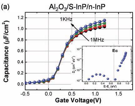
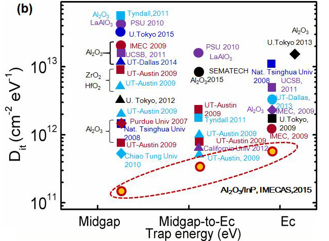
Figure 1: (a) C-V curves and Dit distribution of high-k/InP MOS capacitor made by low temperature ALD technology and surface S-passivation. (b) the Dit of high-k/InP interface is below 2×1011 cm-2eV-1. (Image by IMECAS)
Different from III-V channel, introducing GeOx layer properly between high-k/Ge interface helps to reduce Dit. However, thermal oxidation with high temperature (400~500oC) and atmospheric pressure is proved not suit to the formation of GeOx interface layer. The main reason is that GeO desorption phenomenon above 420 oC is obvious, which then leads to serious degradation of interface properties.
The researchers proposed in-situ cycling ozone oxidation under low temperature (300 oC) during high-k atomic layer deposition to solve the high-k/Ge interface problems. It not only suppresses GeO desorption at high temperature, but also gets ultra-thin GeOx interface layer with high quality by utilizing blocking effect against ozone during high-k dielectric deposition. Through this method, the lowest Dit of high-k/Ge interface decreases to below 2×1011 cm-2eV-1, reaching the world-class level (Figure 2). Optical and electrical characterization also shows that dielectric leakage and defect density in the dielectric both decreased. This method provides promising solution for future application of Ge-MOS devices.
The research was sponsored by the National Science and Technology Major Project of China, 973 Project and National Natural Science Foundation.
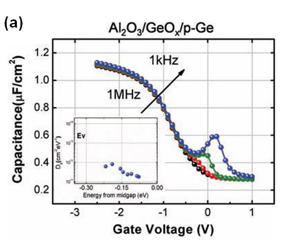
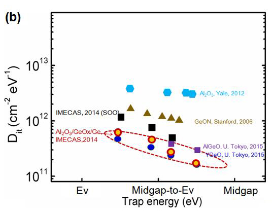
Figure 2: (a) C-V curves and Dit distribution of high-k/Ge MOS capacitor made by in-situ cycling ozone oxidation technology. (b) The lowest Dit of high-k/Ge interface decreases to below 2×1011 cm-2eV-1, reaching the world-class level. (Image by IMECAS)
Reference:
S. K. Wang et. al. Appl. Phys. Express 8 091201 (2015)
X. Yang et. al. Appl. Phys. Lett. 105 092101 (2014)
X. Kong et. al. IEEE Trans. on Electron Devices Volume:62 Issue: 5 1456 (2015)

86-10-68597521 (day)
86-10-68597289 (night)

52 Sanlihe Rd., Xicheng District,
Beijing, China (100864)
Copyright © 2002 - Chinese Academy of Sciences


