Newsroom


A research team led by Prof. LIU Zhiqiang from the Institute of Semiconductors of the Chinese Academy of Sciences, in cooperation with the team led by Prof. GAO Peng from Peking University and the team led by Prof. LIU Zhongfan from Beijing Graphene Institute (BGI), recently realized the concept of "heterogeneous epitaxy" via a van der Walls strategy, a type of nonsymmetrical epitaxy process.
The researchers confirmed the feasibility of nitride epitaxy not limited by the substrate lattice and provided a new idea for the heterogeneous integration of semiconductor materials.
By proposing a nanorod-assisted van der Waals epitaxy technology, they achieved continuous and flat nearly single-crystalline nitride films on an amorphous glass substrate.
After decades of development, the semiconductor industry has entered the "post-Moore era." "Beyond Moore's Law" has ushered in a climax. The development of the semiconductor industry in the future needs to jump out of the original framework and seek new paths.
Faced with these opportunities and challenges, the preparation of basic materials such as wide band-gap semiconductor materials is also gestating breakthroughs. New materials, new processes, and heterogeneous integration will become potentially disruptive technologies in the post-Moore era.
In this study, the researchers used graphene to realize aligned nitride nucleation islands, which inherited crystallinity from the graphene lattice. Then the nitride nucleation islands absorbed adatoms on the graphene surface and evolved into nanorods. Next, nanorods acted as a good template for lattice mismatch alleviation and subsequent coalescence. Thus a smooth nitride film was formed.
According to the researchers, graphene effectively guides the orientation of nitrides, while the designed nanorod template further narrows down the in-plane alignment to three dominant configurations.
"The in-plane dominant orientations are clearly exhibited by atomic resolution high-resolution transmission electron microscopy images at graphene boundaries, which is consistent with density functional theory calculation," said Prof. LIU Zhiqiang, corresponding author of the research.
This work not only experimentally validates the growth of crystalline nitrides on amorphous substrates, but also provides a promising route to the monolithic integration of semiconductors for advanced electronics and photonics.
This method is also suitable for the preparation of high Indium component nitride materials. It proposes a universal method for improving the incorporation of Indium in III-nitrides, which opens up new ideas for the future application of nitrides in the field of new and multifunctional devices.
This research was published online in Science Advances on July 31 in an article entitled "Van der Waals Epitaxy of Nearly Single-Crystalline Nitride Films on Amorphous Graphene-Glass Wafer."
It was funded by the National Key R&D Program of China, the National Natural Science Foundation of China, and the Youth Supporting Program of the Institute of Semiconductors.

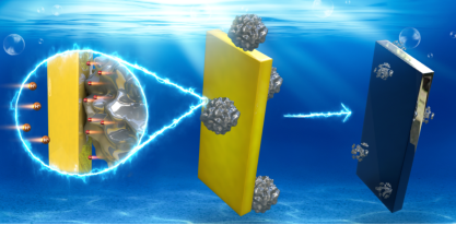
Heteroepitaxy opens a new way for the heterogeneous integration and multifunctional integration of various semiconductors in the post-Moore era. (Image by the Institute of Semiconductors)