
Newsroom


Recently, a research team from the Shanghai Institute of Optics and Fine Mechanics (SIOM) of the Chinese Academy of Sciences (CAS) numerically simulated and experimentally demonstrated a pixelated metasurface based on the silicon-on-insulated (SOI) wafer.
According to the researchers, the metasurface can realize detection of full-Stokes polarization vectors in near infrared. The results were published on Photonics Research on March 31.
Focal plane imaging is a new polarization imaging technology developed in recent years, which mainly relies on pixelated metasurface and charge coupled device (CCD) to detect the polarization component of incident light.
At present, the polarization imaging technology can only detect linear polarization component instead of circular polarization component. The main reason is that the pixel unit lacks the circular polarizer, especially one that can be integrated with a linear polarizer on a single chip. Current circularly polarized films have some disadvantages, such as low circular dichroism (CD), low transmission of circularly polarized light, and difficulty in fabrication. Therefore, the search and preparation of high performance pixelated metasurface that can realize full-Stokes vector detection is the focus of researchers.
The team proposed a high-performance pixelated metasurface to detect the full Stokes vector polarization of near-infrared incident light. Each pixel unit consists of a circular polarizer with a two-dimensional structure and three linear polarizers with the same structure parameters and different gate line directions.
Therefore, all the polarization components of the incident light can be detected by a single exposure. Two-dimensional circular polarizer not only has high circular dichroism, but also is easy to integrate with a linear polarizer.
In addition, the metasurface element is based on SOI, which not only has a high transmission to linearly and circularly polarized light, but also provides the feasibility for the integration with CCD in the subsequent polarization imaging.
In the experiment, the pixelated metasurface was fabricated by the combination of an electron beam exposure system and inductively coupled plasma etching technology. The average transmittance of TM polarized light in the 1.47-1.6 μm wavelength band was about 75%, and the extinction ratio was more than 20dB. The measured average transmission of right-handed circularly polarized light in the 1.48-1.6 μm wavelength band was greater than 80%, and the maximum of CD was up to 70% at wavelength of 1.6 μm, which can meet the requirements of most applications.
The research was supported by the National Nature Science Foundation of China, the International Science and Technology Cooperation Programme, the Shanghai Sailing Program, and the University Scientific Research Foundation of Jiangsu Province.
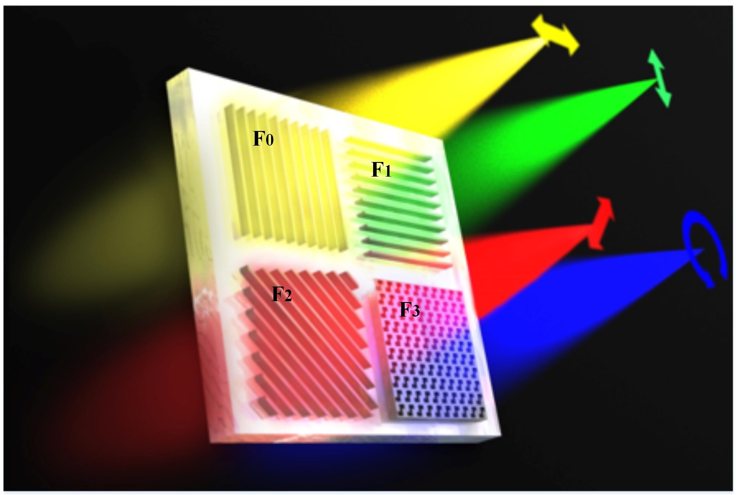
Three-dimensional schematic of the pixel unit. The colors are used only for distinguishment of the image and bear no wavelength information. (F0, F1, F2) and F3 represent linear polarizers and circular polarizer, respectively. (Image by SIOM)
