
Newsroom


A research team led by Prof. REN Wencai from the Institute of Metal Research (IMR) of the Chinese Academy of Sciences has achieved the wafer-scale epitaxial growth of monolayer MoSi2N4 single crystals, a high-performance p-type two-dimensional (2D) semiconductor.
Their findings, published on July 8 in Nature Materials, mark a significant step toward realizing complementary metal-oxide-semiconductor (CMOS) integrated circuits based on 2D materials.
As electronic devices continue to shrink, conventional semiconductors such as silicon face fundamental physical bottlenecks including short-channel effects. Van der Waals layered 2D semiconductors, with their atomically thin thickness and dangling-bond-free surfaces, offer compelling advantages for sub-5-nanometer technology nodes. While various n-type 2D semiconductors including MoS2 and WS2 have been successfully prepared as wafer-scale single crystals, p-type counterparts that combine high mobility and excellent stability remain extremely scarce, and their single-crystal wafer growth has proven even more challenging.
In 2020, the researchers pioneered the creation of the p-type 2D semiconductor MoSi2N4 by introducing silicon into a non-layered molybdenum nitride growth system. This established the MA2Z4 family of van der Waals layered materials. Monolayer MoSi2N4 exhibits a bandgap comparable to that of MoS2, but surpasses it in theoretical carrier mobility, thermal conductivity, Young's modulus, and fracture strength, with exceptional stability. Until now, however, only polycrystalline MoSi2N4 films had been experimentally attainable. Grain boundaries severely degrade electrical transport performance and compromise film integrity during transfer.
To overcome this challenge, the researchers developed a chemical vapor deposition approach using Cu(111) single crystals enriched with Mo and Si atoms as the growth substrate. They found that the <110> steps on the Cu(111) substrate promote the oriented nucleation of monolayer MoSi2N4 domains in a single orientation, enabling seamless stitching into a continuous single-crystal film.
The resulting monolayer MoSi2N4 exhibits outstanding crystalline quality, with an intrinsic carrier mobility reaching 154 cm2 V-1 s-1. Field-effect transistor arrays fabricated from this material deliver excellent electrical performance, including an on/off ratio of approximately 3.8 ± 1.4 × 10⁶ and an on-state current density of up to 17.96 μA μm-1 at a channel length of 1 μm. These arrays also demonstrate superior stability compared to monolayer WSe2-based devices.
Furthermore, this method is versatile and can be used to grow monolayer WSi2N4 single crystals on a wafer scale.
This work establishes a highly promising p-type 2D semiconductor platform for future integrated circuits and provides a general strategy for wafer-scale, single-crystal growth of other 2D materials. This advances their applications in electronics and information technology.
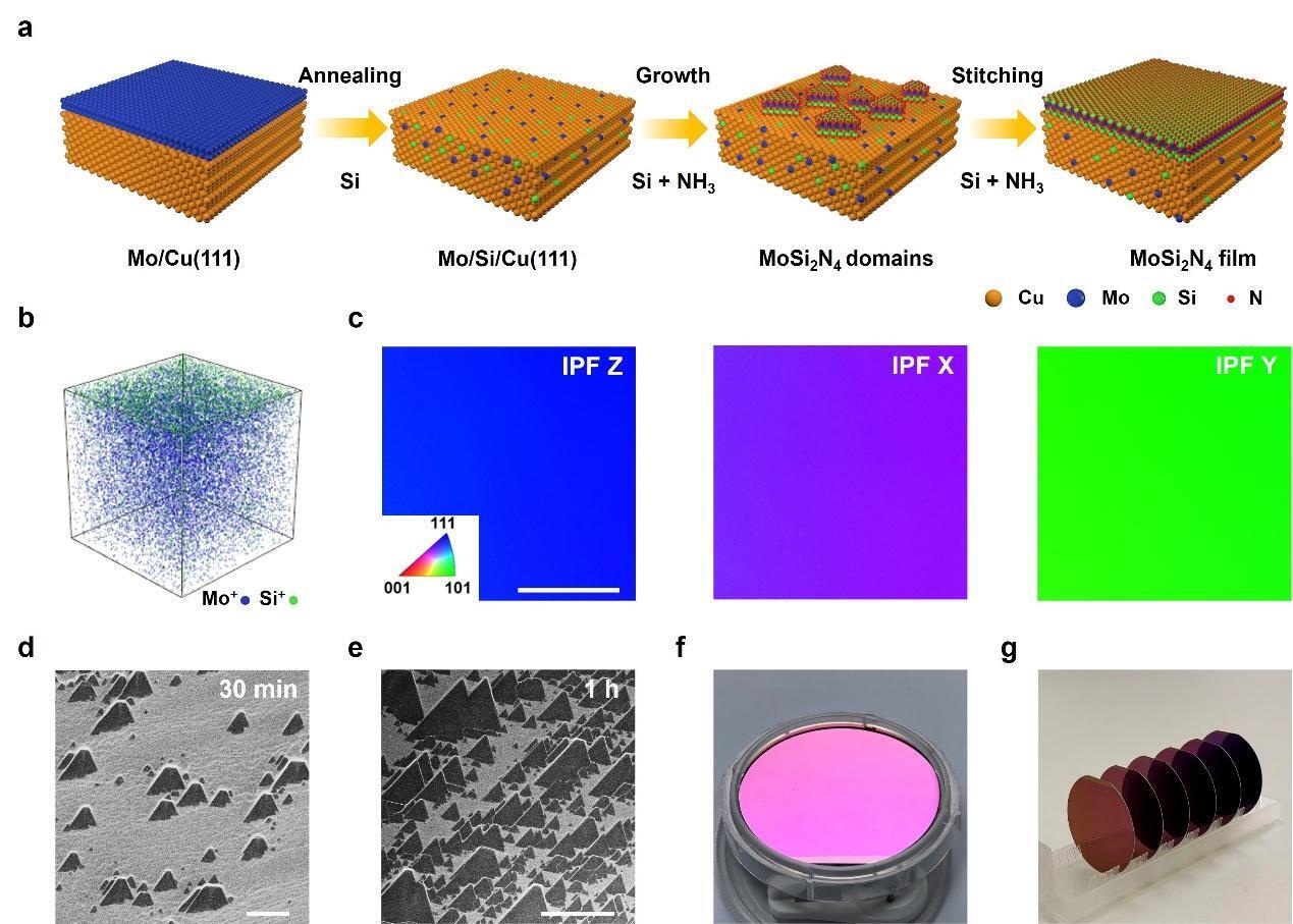
Growth of monolayer MoSi₂N₄ single-crystal wafers. (Image by IMR)
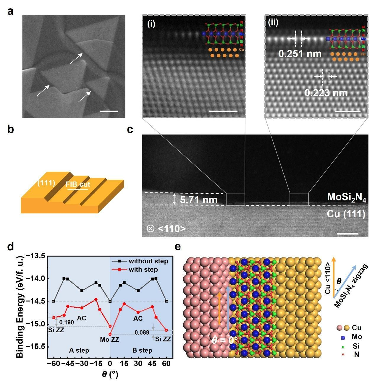
Single-orientation nucleation mechanism of monolayer MoSi2N4 induced by surface steps on Cu(111) single crystals. (Image by IMR)
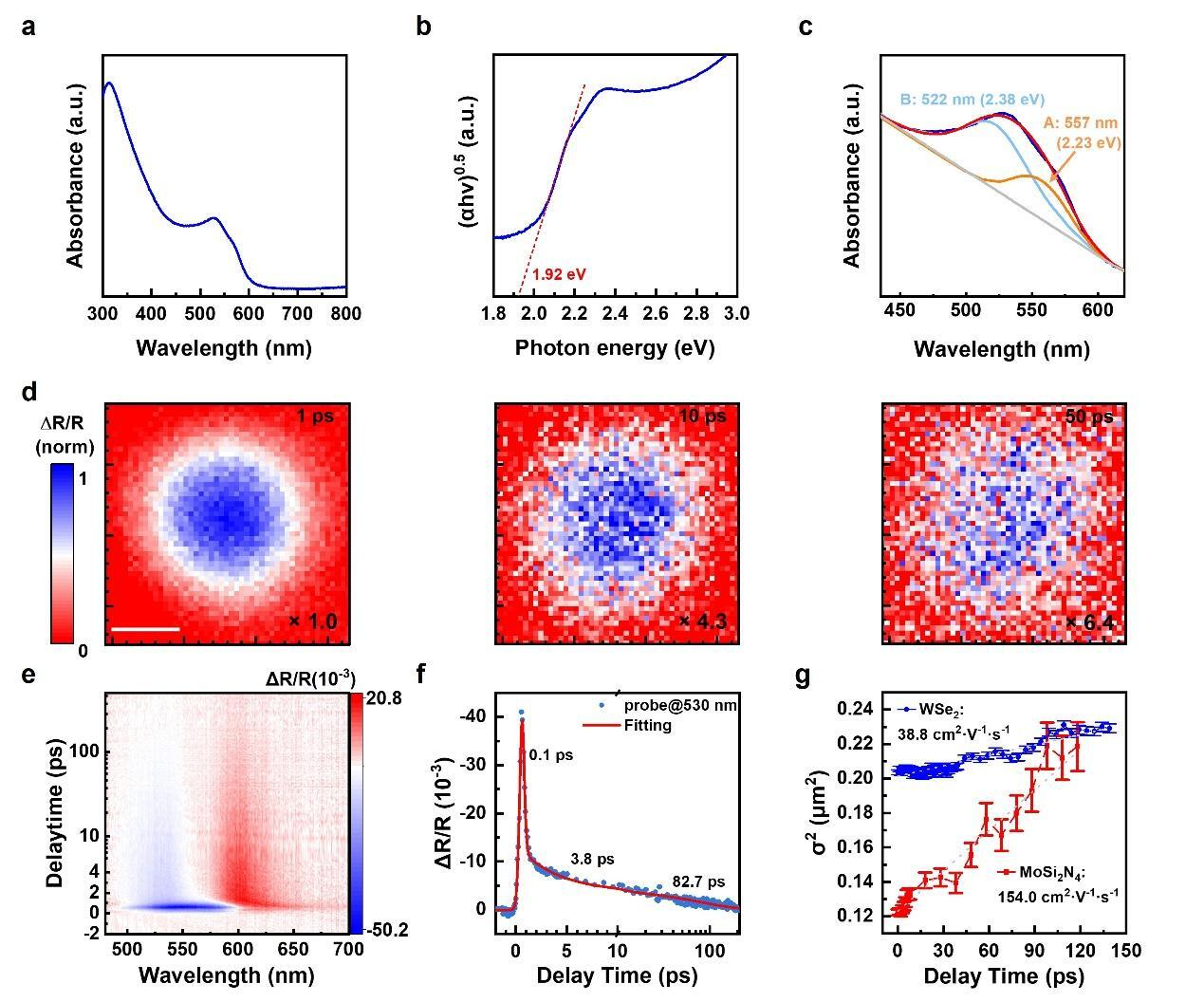
Optical characterization of monolayer MoSi2N4 single crystals. (Image by IMR)
