
Recently, the research group led by Prof. FEI Guangtao, working with Institute of Solid State Physics, Hefei Institutes of Physical Science, has made progress in photoelectric properties of W-doped ordered Vanadium Oxide(VO2) nanowire arrays, and the related research results have been published in Applied Surface Science.
Thanks to high resistance temperature coefficient and excellent photothermal effect, VO2 has great potential application prospects in infrared detection. However, the infrared detection of vanadium oxide mainly focuses on one dimensional single nanowires.
Although these single nanowires have narrow band gap, good crystallinity and high specific surface area, the effective illumination area of a single nanowire is very small and the photocurrent generated is very low, which limits its application.
Therefore, the ordered arrangement of single nanowires can not only bring good photoelectric properties of the device, but also increase the effective illumination area to the maximum extent.
Because of the integration effect of single nanowires and the ordered arrangement of the single nanowires, less transmission obstacles can help the device obtain higher photocurrent values, thus achieving excellent photoelectric response performance.
Otherwise, element doping has many advantages as semiconductors, such as reducing photogenerated electron hole pair recombination, increasing electrical conductivity, free carrier concentration and carrier lifetime, for which it is considered to be an effective method to improve the photoresponse of photodetectors.
Looking at this, XIE Binghe, a graduate student of FEI's team has prepared a high quality two-dimensional ordered W-doped VO2(M) nanowire array.
The ordered W-doped nanowire array exhibits a rapid infrared response of high sensitivity in milliseconds and responsivity of 21.4 mA/W. Compared with the pure VO2(M) nanowire array detector (the responsivity is 0.29 mA/W), the responsivity is increased by nearly two orders of magnitude.
Their study may provide a direct and convenient path to design high performance optoelectronic devices in the future.
The above research was supported by the National 973 Program, the National Natural Science Foundation and the Director of the Institute of solid Physics of the Chinese Academy of Sciences.
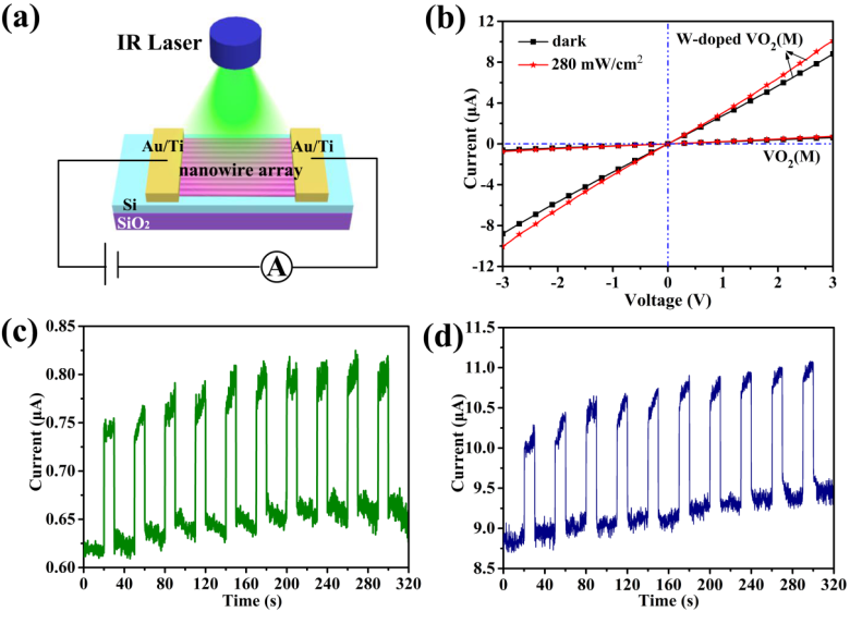
Fig 1. The IR photoelectric response without and with W-doped VO2(M) nanowire array. (a) The schematic diagram of the photoelectric measurement of the nanowire array.(b) Typical Current–voltage (I–V) curves of the pure VO2(M) as well as W-doped nanowire array in dark and under IR laser illumination with light intensity of 280 mW/cm2.(c), (d) Current–time (I–t) curves of pure VO2(M) as well as W-doped VO2(M) nanowire array devices at a voltage of 3 V during on-off switching tests under the pulse IR laserillumination with light intensity of 280 mW/cm2. (Image by XIE Binghe)

Fig 2. (a) Photocurrent rise and decay of the as-prepared photodetector device under an IR laser (b) SEM image of W-doped VO2(M) nanowire array. (Image by XIE Binghe)

86-10-68597521 (day)
86-10-68597289 (night)

86-10-68511095 (day)
86-10-68512458 (night)

cas_en@cas.cn

52 Sanlihe Rd., Xicheng District,
Beijing, China (100864)
Copyright © 2002 - Chinese Academy of Sciences


