

Introducing new channel materials lays the groundwork for slashing the power consumption per transistor BY SHENGKAI WANG FROM THE INSTITUTE OF MICROELECTRONICS AT CHINESE ACADEMY OF SCIENCES
Back in the 1990s, many families would fork out on a new computer every year or so. Occasionally, they would do this because their current PC had stopped working; but more often they parted with their cash to get their hands on a machine that was faster, and capable of running more powerful software.
Fast-forward to today, and a similar state of affairs is at play. Now it is individuals rather than families that are parting with their earnings, and they are splashing out on better mobiles rather than new desktop PCs.
In both of these eras, advances in the performance of the microprocessor underpinned improvements in consumer hardware. Since the 1970s, transistors have got far better, while getting far smaller.
These phenomenal advances in performance will have come as no surprise to Gordon Moore, co-founder of Intel. Back in 1965 he predicted that the number of transistors on a chip will double roughly every two years.
This rate of progress, which is described by Moore’s Law, has largely been driven by evolutionary progress in the basic technology – a silicon transistor sporting a silicon dioxide dielectric beneath the gate. However, to keep pace with Moore’s Law during the last decade, this device has had to undergo some modifications, such as the introduction of strained silicon-on-insulator structures, high-k/metal gate technology and non-planar transistor architectures.
Despite these refinements to silicon CMOS, the traditional advances in power consumption per transistor are stalling. This is a major concern, because rising smartphone sales have led to a shifting of priorities for the silicon IC – gains in performance are still valued, but more than ever before, a fall in power consumption per transistor must occur with every new node in order to ensure an acceptable battery life for the handset.
The well-trodden path to realising more efficient transistors is to trim their operating voltage. Today it stands at 0.8-0.9 V, and the aim is to drive this down to 0.5 V.
One promising way to do this is to rip out the silicon channel and replace it with a material that transports carriers at higher speeds. Success hinges on replicating the high material quality found in the traditional pairing of silicon and SiO2, a combination that allows charge carriers to pass through the channel without undergoing strong scattering.
With silicon, the electron mobility is a modest 1400 cm2 V-1 s-1, while for holes it is just 450 cm2 V-1 s-1. To go to higher speeds, this material could be replaced with a combination of III-V and group IV materials, which are strong candidates for future technology nodes. Of particular promise for next-generation logic is the combination of InGaAs, which could sit at the heart of n-type transistors, thanks to its electron mobility that can hit 10,000 cm2 V-1 s-1; and germanium, which could provide p-type transistors with a hole mobility in excess of 1900 cm2 V-1 s-1.
Before foundries can churn out hybrid, dual-channel CMOS circuits featuring very-large-scale integration (VLSI), researchers in this field must find answers to several important questions. They include: How do you build high-quality interfaces that are comparable to those of SiO2 and silicon? How do you form high-mobility channels with good crystalline quality on a silicon substrate? And how do you build nano-scaled devices based on III-Vs and germanium that are compatible with VLSI?
To try and find the answers to these questions, the Chinese government is backing a programme involving researchers from four institutions: the Institute of Semiconductors of the Chinese Academy of Sciences (CAS), Tsinghua University, the Institute of Microelectronics of CAS, and Peking University. Efforts by this team, which we are a part of, are paying dividends. Five years into an on-going fruitful collaboration, we have succeeded in developing novel engineered substrates and process technologies for high-volume, silicon foundry manufacturing of VLSI circuits featuring compound semiconductor materials (see Figure 1 for an overview of the roles of all the institutions involved in this project).
Gate stack engineering
One of the great strengths of the conventional transistor is the high quality of the interface between silicon and its native oxide. This enables suppression of channel scattering, which could arise from interface traps, and it ensures that MOSFETs produce a nearly ideal sub-threshold swing of 60 mV/dec. Thanks to this steep sub-threshold swing, the operating voltage can be trimmed while maintaining device performance.
It is not easy to replicate the quality of the silicon-SiO2 gate stacks with germanium – and with III-Vs it is even harder. The interfaces between a high-k dielectric and either germanium or a III-V have a higher thermodynamic instability than those formed from the traditional pairing of silicon and SiO2, and this increases the interface trap density by one-to-two orders of magnitude (typical values are 1012 - 1013 cm-2 eV-1). However, efforts by our group at the Institute of Microelectronics of CAS have shown that thermodynamic methods can address these interfacial issues.
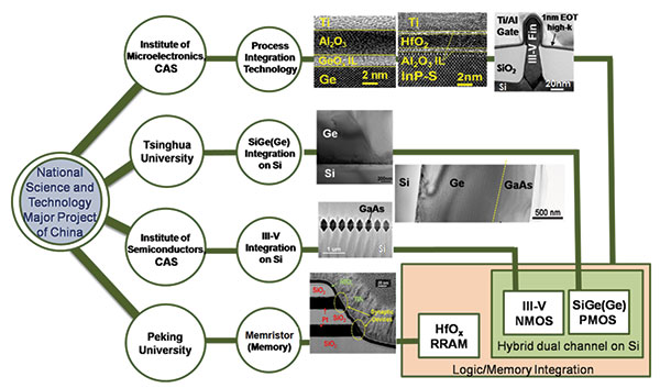
Figure. 1. Supported by the National Science and Technology Major Project of China, four institutions are working together in a project entitled ‘Integration Technology for Silicon Based High Mobility Materials and Novel Devices’ to develop technologies for next-generation ICs. Researchers at Tsinghua University are focusing on the integration and realization of high quality SiGe or germanium-on-silicon, while a team from the Institute of Semiconductors of CAS is grappling with how to integrate III-Vs with silicon; the Peking University team is concentrating on the memristor development using HfOx-based resistive random-access memory (RRAM); and the team from the Institute of Microelectronics of CAS is working on process integration technology, including the high- stack engineering, and process integration technology development.
Our team has formed NMOS devices that feature an InGaAs channel and a thin InP barrier. With this barrier the channel can be kept apart from the high-k oxide interface, leading to higher electron mobility in the channel.
To prevent thermal damage to the devices, we use a low-temperature process to form the gate-stack. This process takes place at 300°C, and is based on the atomic layer deposition of Al2O3 onto a sulphur-passivated InP surface. By carrying out deposition at significantly below 350°C, the temperature at which degradation of the high-κ/InP interface kicks in, we avoid emitting phosphorus atoms from the substrate.
The performance of our transistors is very encouraging. According to capacitance-voltage measurements at a range of frequencies, the interface trap density is 1.2 x 1011cm-2 eV-1. To our knowledge, that is the lowest value ever reported for high-k/InP stacks.
Damage from high-temperature annealing is a common problem as it also degrades interfaces between germanium and high-k dielectrics. To prevent this from occurring, we have inserted a high quality interfacial GeOx layer between the high-k dielectric and the germanium substrate. We introduce this with a cycling ozone oxidation method, which involves repeatedly depositing Al2O3 via atomic layer deposition and then performing in-situ ozone oxidation at about 300°C. Transistors that result have a very low density of interface traps, and capacitance-voltage characteristics that are dispersion free (see Figure 2 (b)).
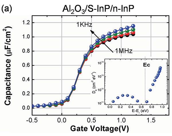

Figure 2. (a) Room-temperature multi-frequency capacitance-voltage characteristics of an Al/Al2O3/n-InP structure fabricated via a low-temperature process. The inset shows the corresponding distribution of interface trap densities across the bandgap. (b) Room-temperature, multi-frequency, capacitance-voltage characteristics of Ti/Al2O3/GeOx/p-Ge fabricated by cycling ozone oxidation. The inset shows the corresponding distribution of interface trap densities across the bandgap.
Our efforts at developing high-quality interfaces between a high-κ dielectric and epilayers of either germanium or InP have set the foundations for making high-speed n-type and p-type transistors that are free from significant scattering at interface traps. To showcase the potential of these devices, we have fabricated enhance-mode, 400 nm-long ultra-thin body MOSFETs that feature an InGaAs channel and an InP barrier. These devices deliver a very promising performance, including a sub-threshold swing of 80 mV/dec and a drain-induced barrier lowering that is typically 35 mV/V (see Figure 3).
Hetero-integration
The microelectronic industry is preparing itself for some colossal changes during the coming years. They will not, however, include a change in substrate. So, to enable III-Vs and IV-IVs to be integrated in CMOS production, these materials will have to be formed on a silicon substrate. This is not trivial, because the crystalline structures of germanium and the III-Vs differ from that of silicon.
Our colleagues at Tsinghua University have tackled this issue by developing a process for forming SiGe and germanium on silicon. They employ a cyclical approach; in the case of germanium this involves the growth of this material directly on a silicon (001) substrate at less than 400°C, followed by deposition at a far higher temperature, which can be between 600-670°C.
Low-temperature growth generates germanium monolayer islands. This is good news, because it suppresses further island growth and it supports a layer-by-layer growth mode. Note that care is needed to not drop the temperature too low, because this would hamper the formation of a smooth layer with good crystallinity (see Figure 4).
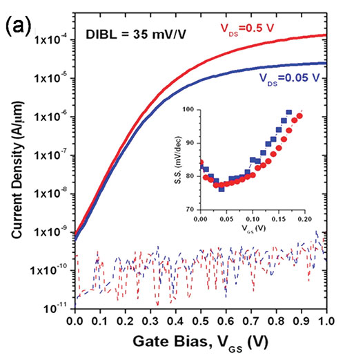
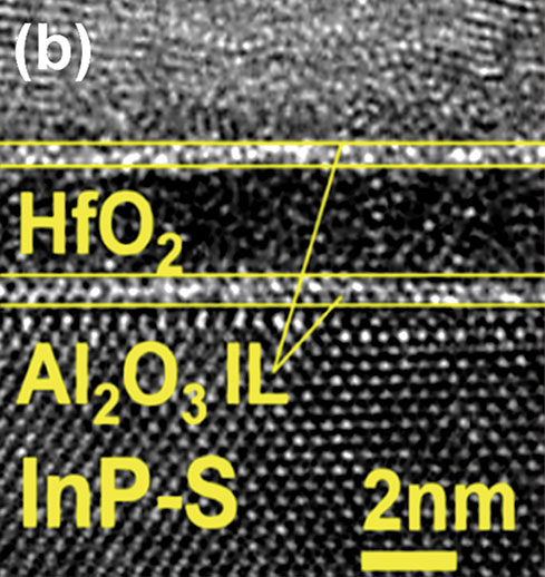
Figure 3. (a) Current-voltage characteristics for a 400 nm-long, enhance-mode, ultra-thin body nMOSFET featuring an InGaAs channel and an InP barrier layer. The on-off ratio is over 105, the average sub-threshold swing factor is typically 80mV/dec, and the drain-induced barrier lowering is around 35mV/V. (b) Cross-sectional transmission electron microscopy image of the optimized Ti/HfO2/Al2O3/InP/InGaAs gate stack.
The low-temperature growth does have a downside, as it leads to a very high density of dislocations – they are typically 108 - 109 cm-2 – but this does allow high-temperature growth that follows to relax the maximum amount of strain. When the film is subsequently annealed under hydrogen at 750-825°C, dislocations glide and annihilate. This decreases their density and increases the degree of relaxation in the material. Films with a surface roughness of typically 0.5 nm result, which have a threading dislocation density below 105 cm-2.
Within the programme, efforts at integrating III-Vs and silicon have been led by a team at the Institute of Semiconductors of CAS. They have adopted a two-pronged approach, pursuing direct epitaxy of GaAs on germanium/silicon virtual substrates and aspect ratio trapping (ART).

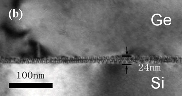
Figure 4. (a) Cycling between low-temperature and high-temperature growth of germanium leads to smooth, high-quality films. (b) Cross-sectional transmission electron microscopy reveals misfit dislocations trapped at the interface between germanium and silicon.
The direct epitaxy approach involves MOCVD of device-quality GaAs on germanium-on-miscut
silicon. A high-quality top layer is realised with a two-step approach: a thin buffer is deposited at 360°C, followed by higher temperature growth; and polishing is then performed, followed by a second epitaxial growth. Merits of the thin buffer include the suppression of anti-phase boundaries and threading dislocations − the latter can reach 2.3 × 105 cm-2, according to experiments involving potassium hydroxide etching.
Inspection of these GaAs-on-silicon films with a transmission electron microscope reveals the high quality in the top layers of the III-V (see Figure 5). The surface roughness of these films can be below 1 nm, which is comparable with that of homo-epitaxial GaAs layers. The low density of defects in these epilayers, and their smooth surfaces, are attributes that are needed for making logic devices.
The biggest challenge for integrating a III-V on large silicon substrates is the significant lattice mismatch between the two materials. ART offers an elegant, cost-effective solution to this problem, and has been employed by researchers at the Institute of Semiconductors to realise selective area growth in ‘V-shaped’ trenches.
Efforts in this direction began by forming GaAs on silicon (001) using a two-step MOCVD process. Following on from this, high-quality films of InP, InGaAs, and InAs are sequentially grown in trenches lined with a GaAs buffer layer. The material quality of the films is very high, according to transmission electron microscopy (see Figure 6). This approach shows great promise for the realization of high-mobility devices for future CMOS technology nodes.
Building devices
Success in our programme has laid the groundwork for making devices. Well-tailored interfaces and high-quality hetero-material integration technology form the starting point for our construction of high-performance, low-power-consumption logic devices. We are also well positioned for trying to realise logic-memory integration on a silicon platform.
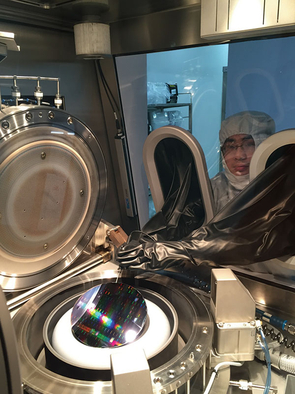
In 2014, our team at the Institute of Microelectronics CAS made our first attempt at fabricating small-sized III-V MOSFETs in our 8-inch line, which is intended for research and development. We found that a well-developed replaced-silicon fin technology held the key to realizing a 20 nm-width high-quality InGaAs-fin with an InP barrier layer. During this marriage of materials, which was accomplished on 8-inch silicon, dislocations were restricted to the SiO2 trench, resulting in a high-quality ‘head’ (see Figure 7). Despite deploying an optimised, high-k dielectric with an equivalent-oxide thickness of 1 nm, and a Ti/Al gate, transistors were hampered by issues arising from process integration, such as bulk leakage. We are working to address these weaknesses.
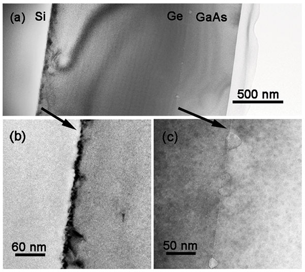
Figure 5. Cross-sectional transmission electron microscopy images highlight the high-quality of the of GaAs/germanium/silicon stack (a), and the interfaces between germanium and silicon (b), and GaAs and germanium (c).
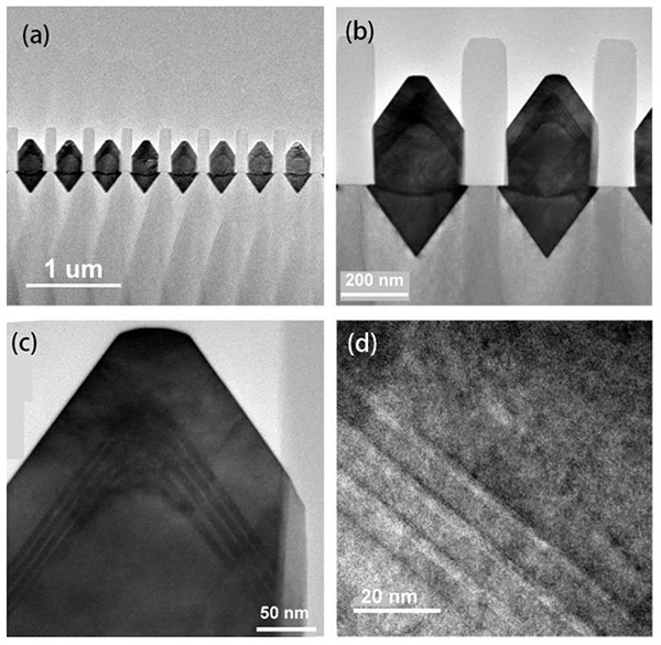
Figure 6. Transmission electron microscopy shows InGaAs multi-quantum wells that are formed in trenches by aspect ratio trapping, using InP and GaAs layers (a) and (b). The wells are uniform, according to images (c) and (d).
Our colleagues at Tsinghua University are focusing on PMOS devices, and are pioneering an architecture that promises to abolish the trade-off between performance and power consumption. This team has fabricated junctionless germanium-nanowire transistors on an extremely thin germanium-on-insulator substrate by carefully controlling wet etching. The devices that result have gate lengths and widths below 100 nm, and exhibit good electrical characteristics, such as an on-off drive current ratio of 105 at a drain voltage of -1V. These transistors are very promising candidates for PMOS devices in future microprocessors (see Figure 8). To make ICs, PMOS and NMOS devices must be formed side by side on the same wafer. In our programme, we grow germanium on silicon, and then add III-Vs to the germanium-on-silicon substrates by either direct epitaxy or ART. Germanium-PMOS transistors are formed first, because they need relatively high temperatures for p-type dopant activation and gate-stack annealing, such as typically 400°C. Fabrication of III-V NMOS devices follow, using InGaAs and an InP barrier layer. Dopants in these n-type devices do not require activation, because the source and the drain are formed by etching the epitaxy layer.
Another avenue explored by our programme is the integration of logic-memory for the post 10 nm node. The high mobility of carriers in III-V and germanium channels enables high drive currents at relatively low operating voltages − and this makes this hybrid material approach attractive for both the construction of logic-memory integration blocks and the production of advanced memory devices.
One attractive candidate for next-generation microsystems is the hybrid crossbar memristor − also known as resistive random access memory − that is formed with a high-mobility MOS transistor array. Within our programme, a partnership between our group and a team from Peking University has developed an integration process for a HfO2-based memristor and a germanium-based pMOS transistor. This effort involved fabricating a memristor with a Pt/HfO2/Al2O3/TaN structure on the drain side of a germanium-based pMOS transistor. With this device, turning the pMOS transistor to its on-state enables operation of the memristor (see Figure 9 for related current-voltage curves).
Our programme continues, and we are working towards several important goals. They include using our successes to date to demonstrate a dual-channel CMOS unit, and investigating in more detail device reliability, with a focus on the gate stack in both p-type and n-type transistors. Last but not least, we will start to consider making non-planar devices with germanium and III-V channels, as this is a very promising option for maintaining the march of Moore’s law. (Compound Semiconductor)
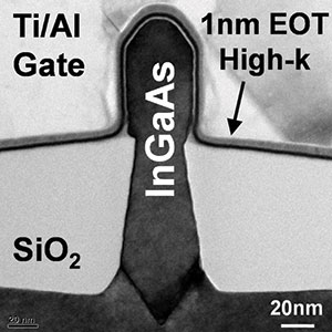
Figure 7. Cross-sectional transmission electron microscopy highlights one of the major successes of the Chinese program: fabrication of a 20 nm-width, high-quality InGaAs-fin (with InP barrier layer) on an 8-inch silicon wafer.
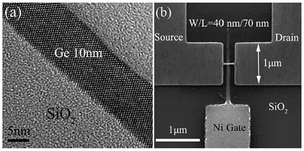
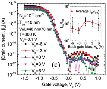
Figure 8. (a) Cross-sectional transmission electron microscopy of an ultra-thin body, germanium-on-insulator structure with a germanium film thinned to 10 nm. (b) Scanning electron microscopy of an ultra-thin body, germanium-on-insulator-based junction nanowire transistor with a 70 nm gate length and a channel width of 40 nm. (c) The back gate bias influences the current-voltage characteristics of this device. The inset shows the influence of bias voltage on the on-off current ratio at a drain voltage of -0.1 V.

Figure 9. A typical current-voltage curve of HfO2-based resistive switching device; the current was complied by a germanium-PMOS transistor. ‘Set’ means resistive switching from a high-resistive state to low-resistive state. ‘Reset’ means resistive switching from a low-resistive state to high-resistive state.

86-10-68597521 (day)
86-10-68597289 (night)

86-10-68511095 (day)
86-10-68512458 (night)

cas_en@cas.cn

52 Sanlihe Rd., Xicheng District,
Beijing, China (100864)
Copyright © 2002 - Chinese Academy of Sciences


